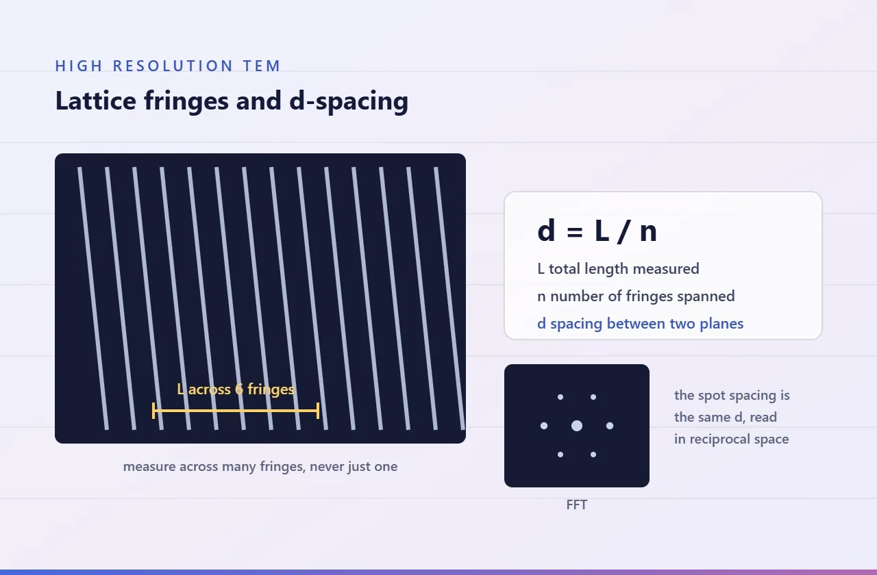
SEM stands for Scanning Electron Microscopy or Scanning Electron Microscope. It is an advanced technique used to study the surface of a material at very high magnification.
In simple words, SEM helps us see what a sample looks like at the micro or nano level.
It is widely used by researchers, students, startups, and industries to study surface morphology, particles, cracks, pores, coatings, fibers, fractures, and microstructure.
SEM is commonly used in fields like materials science, nanotechnology, metallurgy, ceramics, polymers, pharmaceuticals, cement, coatings, electronics, batteries, and failure analysis.
How Does SEM Work?
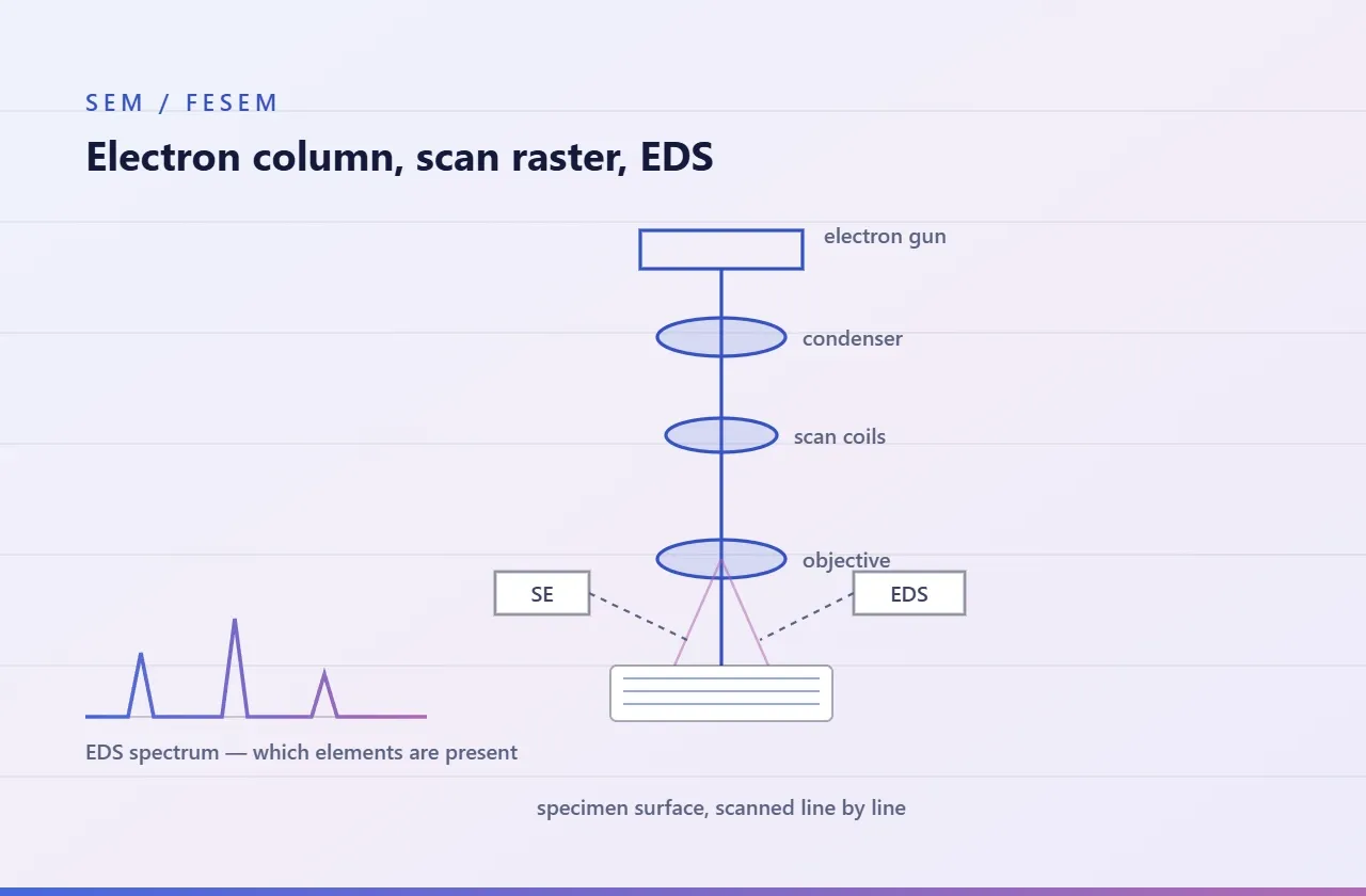
A normal microscope uses light to see a sample. SEM uses a focused beam of electrons.
When the electron beam hits the sample surface, different signals are generated. These signals are collected and converted into a high-resolution image.
This image shows surface details that are not visible through a normal optical microscope.
Because of this, SEM is very useful when researchers want to understand fine surface features, small particles, cracks, or defects.
What Can SEM Show?
SEM mainly gives information about the surface of the sample.
It can help observe:
Surface morphology
Particle shape and size
Cracks and pores
Grain structure
Coating quality
Fiber structure
Fracture surface
Surface roughness
Defects and contamination
Microstructure of materials
For example, if a powder sample is analyzed by SEM, it can show whether particles are spherical, irregular, rod-shaped, plate-like, or agglomerated.
If a coating sample is analyzed, SEM can show whether the coating is smooth, cracked, porous, or non-uniform.
If a broken metal or polymer part is analyzed, SEM can help study the fracture surface and possible reason for failure.
Key SEM Testing Capabilities
SEM is not only used for taking images. It supports many important testing and characterization needs.
1. Surface Morphology Analysis
SEM helps understand the surface texture of a material. It can show whether the surface is smooth, rough, porous, cracked, layered, or fibrous.
This is useful in coatings, polymers, metals, ceramics, composites, and nanomaterials.
2. Particle Morphology Analysis
SEM is useful for studying powders, nanoparticles, fillers, catalysts, pigments, and pharmaceutical particles.
It helps observe particle shape, particle size, surface texture, and agglomeration.
3. Crack, Pore, and Defect Identification
SEM can show cracks, pores, voids, and surface defects clearly.
This is useful for quality control, failure analysis, and product improvement.
4. Coating and Thin Film Observation
SEM can be used to check coating quality, surface uniformity, cracks, pinholes, roughness, and film morphology.
In cross-section analysis, SEM may also help observe coating thickness and layer structure.
5. Fracture Surface Analysis
When a material breaks or fails, the fracture surface contains important information.
SEM helps study the type of failure and surface features after fracture. This is useful in metals, polymers, ceramics, composites, and mechanical components.
6. Microstructure Observation
SEM helps observe grains, phases, boundaries, pores, and structural changes in materials.
This is useful for metals, alloys, ceramics, cement materials, composites, and heat-treated samples.
What is SEM-EDS?
Many SEM instruments are attached with EDS.
EDS stands for Energy Dispersive X-ray Spectroscopy.
SEM gives the image of the sample surface. EDS gives elemental information from the selected area of the sample.
For example, if SEM shows a particle or defect, EDS can help identify which elements are present in that selected region.
SEM-EDS can help answer questions like:
Which elements are present in this area?
Is there any contamination?
Is the coating made of expected elements?
Are particles rich in a particular element?
Is there any impurity in the selected region?
However, EDS has one important limitation.
EDS gives local elemental composition from the selected area. It does not always represent the full bulk composition of the entire sample.
For bulk elemental analysis, techniques like XRF or ICP are more suitable.
Common Applications of SEM Testing
SEM is used in many industries and research areas because surface structure strongly affects material performance.
Materials Science
SEM helps study morphology, microstructure, cracks, pores, and processing effects in materials.
Nanotechnology
SEM is used to observe nanoparticles, nanofibers, nano-coatings, and agglomeration.
Metallurgy
SEM helps study grain structure, fracture surface, corrosion, inclusions, and failure behavior.
Polymers and Plastics
SEM can show fracture behavior, filler dispersion, fiber structure, cracks, and surface defects.
Ceramics and Cement
SEM helps observe pores, cracks, grains, hydration products, and microstructure.
Coatings and Thin Films
SEM is used to check coating uniformity, cracks, roughness, pinholes, and surface quality.
Pharmaceuticals
SEM helps study drug particle morphology, powder shape, crystal structure, and surface texture.
Batteries and Energy Materials
SEM is useful for studying electrodes, separators, catalysts, carbon materials, and degradation after use.
Failure Analysis
SEM helps understand why a material cracked, broke, corroded, peeled, or failed during application.
What Samples Can Be Tested by SEM?
SEM can be used for many sample types, such as:
Metals and alloys
Powders and nanoparticles
Polymers and plastics
Ceramics and cement materials
Coatings and thin films
Fibers and composites
Minerals
Fractured parts
Electronic components
Biological samples after proper preparation
The sample should usually be dry, clean, and stable under vacuum.
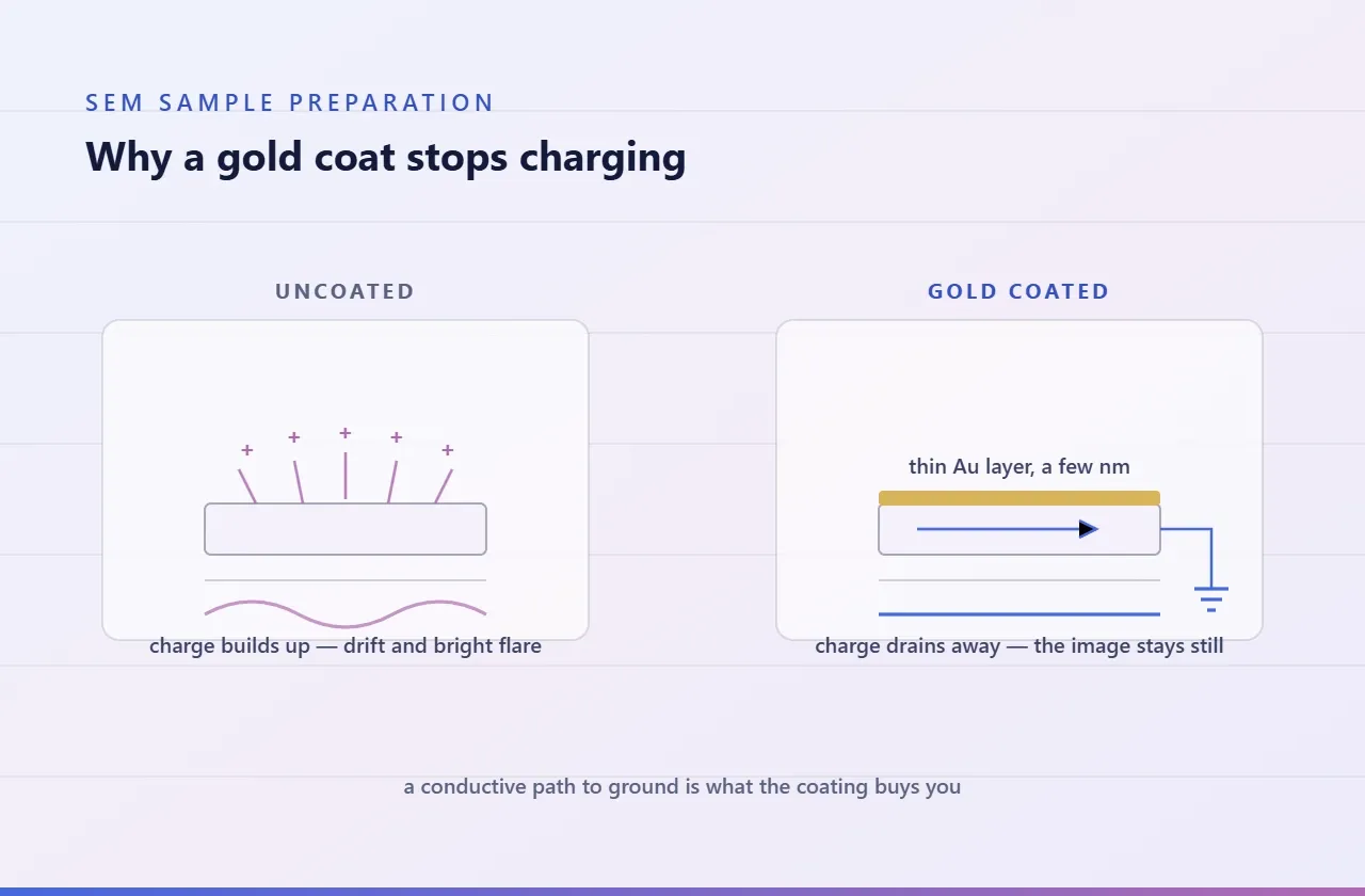
Non-conductive samples may need gold coating or carbon coating before SEM analysis.
Why Gold Coating is Used in SEM
Some samples do not conduct electricity. These are called non-conductive samples.
When such samples are exposed to an electron beam, charge can build up on the surface. This can disturb the SEM image.
Gold coating creates a thin conductive layer on the sample surface. It helps reduce charging and improves image quality.
Gold coating is commonly used for polymers, ceramics, biological samples, and some powder samples.
However, if EDS analysis is required, coating material should be selected carefully because it may also appear in the EDS result.
Limitations of SEM Testing
SEM is a powerful technique, but it has some limitations.
SEM mainly gives surface information.
EDS gives elemental data from selected areas only.
It does not directly give full bulk composition.
Wet samples are usually not suitable without special preparation.
Non-conductive samples may need coating.
Sample preparation can affect the result.
Interpretation needs technical understanding.
So, SEM should be selected based on the purpose of testing.
For surface morphology, SEM is very useful.
For elemental analysis of a selected area, SEM-EDS is useful.
For bulk elemental composition, XRF or ICP may be better.
For phase identification, XRD is more suitable.
SEM vs EDS vs XRF vs XRD
Here is a simple comparison:
SEM shows surface morphology and microstructure.
EDS shows elemental composition from a selected area during SEM analysis.
XRF gives bulk elemental composition of the sample.
XRD identifies crystalline phases present in the sample.
Each technique gives different information. Many times, researchers use more than one technique to understand the sample properly.
Why SEM Testing is Important
SEM testing helps researchers and industries understand materials in detail.
It helps answer practical questions like:
What does the surface look like?
Are there cracks or pores?
What is the particle shape?
Is the coating uniform?
Is there any surface defect?
Why did the material fail?
Is there contamination in a selected area?
How did processing affect the microstructure?
These answers are useful for research, product development, quality control, and failure investigation.
Conclusion
SEM is one of the most useful techniques for surface-level material characterization.
It helps study morphology, particles, cracks, pores, coatings, fibers, fractures, defects, and microstructure at high magnification.
When combined with EDS, SEM can also provide elemental information from selected areas of the sample.
However, SEM and EDS mainly provide local surface-level information. For bulk elemental analysis, XRF or ICP may be more suitable. For phase identification, XRD is useful.
Overall, SEM testing is a powerful tool for researchers, students, startups, and industries who want to understand their material better and improve product performance.
At RNDgrid, we help researchers and industries access SEM, SEM-EDS, and other advanced material characterization facilities through our trusted lab network.